Showing posts with label SMT Technology,Placement machine Models. Show all posts

Tuesday, December 5, 2017

Estimating Pickment Machine Costs refer to BOM Analysis

Estimating Placement Machine Costs refer to BOM Analysis

Since the cost of placement machines accounts for 70% of the production line, it is important to analyze the value of the machine, It can be tempting to try to cut corners in this part of the SMT assembly process, but attempts to save funds in the short-term could cost you in the long run. Some of the productivity headaches we’ve had customers tell us about when they’d tried to “go cheaper” in the past include:

Time lost to excessive changeovers or attempts to optimize setups
Failure to keep pace with output goals
A need to add costly hand assembly for parts the machine didn’t handle
Too much offline time due to service and support issues
It is, however, just as easy to overspend—on capacity, speed, or features you don’t need. The more you invest in a machine, the longer it takes for it to earn its keep. So why waste money on capability you’ll likely never use?

The sweet spot is to achieve payback within a year or so—without incurring additional unexpected costs. At Joysmt, we’ve been able to work with customers to get them a return on their investment in as little as nine months.

It all comes down to maximizing productivity while minimizing investment dollars—something that’s a lot easier to do if you do it all the time, like our team does. Of course, you can try to do it on your own or you can hire a consultant to help you, but did you know that Joysmt offers—free, with no obligation—a full-scale professional analysis of your production requirements and bills of materials (B.O.M.)? For no charge, Joysmt will custom-configure a machine to meet your exact specifications and throughput requirements. What’s more, based on your total budget, we will make recommendations for feeder types, sizes, and quantities to provide optimum performance, minimum changeover, and the quickest return on your investment.


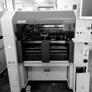
Full-Scale Production Analysis
What does a free Joysmt Production Analysis entail? It starts with one of our experienced team members asking you basic questions about your needs. For example:

What’s the largest PCB you assemble?
What is the smallest component you need to place? How many?
The finest pitch QFP? BGA?
What is the largest component you need to place? How many?
How many different board designs do you have to build?
Are the boards single- or double-sided?
What is the maximum number of unique components on any one side of all of the boards you build?
Is there a lot of component commonality among the various board designs?
How many total component placements are there per board?
For each design, how many boards do you need to assemble per year?
What is the typical size (number of boards) of a production run?
Will your pick and place be used as an in-line machine or in a stand-alone batch configuration?
We’ll also ask you to send along the full B.O.M. for each of your products. (And we're happy to sign an NDA agreement before you send it.) You needn’t worry if your B.O.M. is in a raw format. Our team can usually identify component sizes and packaging from your most basic descriptions by means of our extensive SMD cross-reference.


Feeder capacity, combined with a feeder strategy geared toward optimizing and streamlining setup and job changes, can make the difference between a chronic headache and a smooth-running operation for manufacturers who intended to run several different jobs on a single machine.

All of this information together will help us pass along to you the following information:

The pick and place machine model(s) that will best meet your placement accuracy, range of component sizes, feeder capacity (for either batch or inline configurations), and throughput requirements (CPH)
The minimum number, types, and sizes of feeders you’ll need to build any one of your boards
The number, types, and sizes of feeders you’ll need, optimized for common components across jobs to ensure minimal changeover
Optional cameras or other accessories needed to handle ultra-small, over-sized, or odd-form components
Other accessories and recommendations that can minimize cost and maximize machine utility
Making use of decades of experience evaluating B.O.M.s and custom configuring countless pick and place machines, our equipment experts will carefully review this information with you, along with strategies for simplifying changeovers, streamlining workflow, and reducing your overall pick and place machine cost.

Joysmt provides similar free needs-analysis services for all our major production equipment, including reflow ovens, stencil printers, complete assembly lines, and wave solder machines. Whatever your equipment needs, get in touch with a Joysmt electronics assembly equipment expert today.

Solder wire and paste feature | SMT Technology


Solder voiding is present in the majority solder joints and is generally accepted when the voids are small and the total void content is minimal. X-ray methods are the predominate method for solder void analysis but this method can be quite subjective for non grid array components due to the two dimensional aspects of X-ray images and software limitations. A novel method of making a copper “sandwich” to simulate under lead and under component environs during reflow has been developed and is discussed in detail. This method has enabled quantitative solder paste void analysis for lead free and specialty paste development and process refinement. Profile and paste storage effects on voiding are discussed. Additionally an optimal design and material selection from a solder void standpoint for a heat spreader on a BCC (Bumpered Chip Carrier) has been developed and is discussed.


Solder voids in solder joints are a common occurrence in SMT assemblies. Their origins are not well understood but are typically faulted as a failure of the solder fillet to thoroughly expel flux remnants during the reflow process. The amount of solder voiding can vary significantly within an assembly, between different flux formulations, solder alloys, board and component metalizations. Reflow profiles as well as stencil aperture designs can often affect the overall level of voiding.


Adding to the mystery of solder voiding is a lack of quantitative measurement tools in the industry with few exceptions. BGA void analysis software is one of these exceptions. This software uses gray level pixel analysis to determine the perimeter of the solder sphere and the internal perimeters of the voids. Once the perimeters are established the areas within these structures can be measured and an overall percent voiding can be calculated. This type of measurement works well if the voids are large or found on the outer edges of the sphere but if the void is small and centrally located where the sphere density is the greatest then the void may be invisible due to its relatively similar gray level to the surrounding material. Increasing the X-ray power will reveal the small void but also shrink the measured area of the sphere and yield an inaccurate and inflated percent voiding. This problem is even more complicated in a chip or a leaded component solder joint. When X-raying a completed assembly, internal traces, vias and even components on the backside of the board that intersect the image of the solder joint confound the software algorithms ability to accurately determine the perimeter of the solder joint. In simple terms the X-ray image is two-dimensional and the ideal structure must be symmetrical about the Z-axis such as a box or a cylinder.

Novel Approach

Based on the assumption that the ideal quantitative void measurement method will utilize BGA analysis software and a symmetrical Z-axis reflow structure, the “sandwich” concept was developed.


This a novel approach simulates the worst conditions of a solder joint for voiding, under the component where flux evacuation is the most difficult while maintaining the same reflow thermal environment and metallurgies if desired. This idea was born out of a quest for a quantitative method of determining the percent voiding on a Ceramic Column Grid Array (CCGA)1. In the CCGA the columns are 10/90 Sn/Pb and cover about 45% of the solder fillet. If enough power is used to see through these dense columns, the perimeter of the solder joint is washed out and 55% of the total fillet is invisible. If adequate power is used to see the perimeter of the circular fillet, the area under the columns is invisible. The effort is complicated by column parallax, internal traces and vias as can be seen in Figure 1. With the thought of a column the same diameter as the solder pad that is thin enough to be X-rayed without excessive power, a solder preform was selected. In this application the preform alloy was selected to be the same as the 10/90 columns to minimize the variables that could contribute to solder voiding. Several thicknesses were tested with a 30 mil diameter by 5 mil thick as the final solution.


There were numerous challenges placing these discs. The first problem was a reliable source cup shaped and stacked discs were the first problems to solve. The second problem was the mechanics of actually placing the discs in that the vision systems in the pick and place were never programmed to recognize round components, only components with corners like typical chips. This relegated a “ballistic” pick and place strategy. For this problem a precision matrix tray with cylindrical pockets, each holding one preform, was developed as in Figure 2. Next came improvements to the pick and place nozzle. The stock smallest nozzle OD was the same as the preform. This presented numerous pick problems if the preform was not perfectly centered, occasionally the preform would flip on its edge after pick and crash on placement deforming the preform. Several improvements were made ultimately reducing the nozzle tip down to what would be typical for a 0201 chip as in Figure 3. Reducing the nozzle tip surface area helped eject the preform better in the placement operation.

Assembly of the CCGA test coupons is simple SMT assembly beginning with a “pads only” ceramic coupon to maintain the geometries and pad metalization of the application. This coupon is free of internal traces as in Figure 4. The solder paste is printed through a circular aperture that is 1 mil smaller in diameter than the pad, the preform is placed over the solder paste and then reflowed as in Figure 5. It was established that if the preform was off pad less than 4 mils that it would self-center. Careful attention to Z-axis placement is required to prevent shorting with adjacent preforms.

After assembly the coupon area was X-rayed and quantitative void analysis was performed on the image using off- the-shelf BGA analysis software as in Figure 6. This software provides both total percent voiding and a pass/fail status if any individual void within a structure is larger than a preset number (ie 5%). This technique worked very well for the custom formulated 63/37 Sn/Pb based solder paste or any other alloy with a similar melt point but when tested with lead free (Sn/Ag/Cu, Mp 219°C) it was noticed that the preforms had appeared to melt and partially join the underlying solder paste under test. This was remedied by switching to OFHC copper preforms of identical geometries. For generic paste void benchmarking2 a dedicated pad test area (Figure 7) was included in the Benchmarker II test board. This allows the testing of solder pastes on standard PCB surfaces such as Entek OSP (Organic Solder Protectant) and ENIG (Electroless Nickel Immersion Gold). Quite simply we are making copper sandwiches (Figure 8) that result in cylindrical structures, which permit highly quantitative void analysis with standard BGA analysis software.

rom this data there are clearly different trends for the two materials as well as a significant difference in void behavior between them. The effect of time on Material A is accelerated in cold storage and just the opposite with Material B. Both materials have the exact same source and specifications of the inorganics (powder + additives).


Profile Effects
The effect of the reflow profile can be significant but the magnitude varies greatly from one formulation to another. The following example involves two 63/37 Sn/Pb no clean materials3,4, tested over Entek passivated copper using the copper preforms with the 4 profiles as illustrated in Figure 10. This profile matrix is designed to expose profile sensitivity of a given formulation, in this case relating to voiding. There are two profiles with a ramp style preheat and two with a soak preheat. There are 2 profiles with a peak of 225°C with 60 seconds over liquidous and two hotter profiles with a peak of 240°C with an extended liquidous of 90 seconds. The X-ray data has been compressed into a single “point scale” to facilitate comparisons. These points (100 is best) are calculated .

BGA REWORK|SMT Technology

BGA REWORK

Since the late 1990s ball grid array (BGA) packages have been gaining as a preferred package style for several reasons. Their IO density compared with the previous high density ultra fine pith quad flat packs (QFPs) is such that they have shrunk the necessary footprint on the PCB by a factor of 50%. If we lump the BGA style of package, a high density IO with solder balls for the interconnection in with its stacked version counterpart the POP then this increase in density approaches nearly 100%. The ability to get more done in less space along with shorter trace spacing and length requirements for board layouts using this package style have allowed boards to be clocked at much higher rates


thereby increasing processing speed. In addition the reliability of the placement of BGAs has been high as initially the tin lead solder balls “self centered” on the pads during reflow. Lastly the reliability

of BGA packages has been increased with the use of underfills, the use of specialty flex solder balls and even solder columns with integrated springs.

The increased use of BGAs and the underlying trend of ever-smaller package sizes, finer pitches and their placement on to ever denser printed circuit boards has led to greater and greater challenges in BGA rework. In addition to these challenges there are many others that have made the job of BGA rework technicians more and more difficult. One of the trends in making BGA rework more difficult is their ever-increasing usage in handheld device. Due to the drop test requirements of these products

in many cases the BGAs and other higher density devices need to be underfilled. Underfilled BGAs have the challenge of the tacky material “squirt out” causing solder shorts underneath the BGA. In

addition, the tacky nature of this material tends to lift pads as well as destroying the underlying solder mask underneath he BGA. This makes the BGA rework even more challenging. The ever-thinning device packages of BGAs cause the packages to warp. This too makes BGA rework difficult.

While large packages with large-sized pitches placed on sparsely populated printed circuit boards made BGAs simple to remove and replace, BGA rework today requires a greater level of machine sophistication. With pitches down in to the 0.3mm areas and package sizes routinely under 10 x

10mm placement with a vision system using a highly precise and repeatable XY motion system is required. Placement accuracies for today’s BGA rework need to be in the less than a 1mil tolerance

range. In addition with the lead free packages the rework system now require sophisticated temperature control with programmable multi zone bottom heaters, nitrogen capability and low flow rates at the air nozzle. In addition to the rework equipment set the inspection equipment needs to be of a higher capability. X-ray inspection equipment with very small spot sizes is a requirement for BGA inspection post BGA rework. The ability to measure the sphericity of the solder balls, the solder ball diameter, the ability to shoot through RF shields as well as higher density ground planes is now a necessity for the x-ray equipment requirements for BGA rework. Also the endoscope is a necessity for checking the ball collapse, the surface of the BGA ball post reflow, the wetting action as well as other attributes is important in BGA rework.

In addition to the equipment requirements for modern day BGA rework, the skill level, dexterity and process knowledge of the rework technicians working on BGA rework is even more demanding today. The BGA rework technician needs to understand reflow profiles in order to deal with printed circuit boards with a high density of ground planes. The BGA rework technician must also understand flux chemistries and how this impacts the kind of cleaning which can be done underneath the device. The BGA rework technician must also be able to understand how a variety of conformal coatings can be removed from the PCB as well as underneath the BGA. BGA rework technicians must also understand how device which neighbor the BGA to be reworked can or could be impacted by the BGA rework process profile.

As BGA packages have become more widely-accepted the BGA rework process has become more difficult. This has meant that both the equipment used in BGA rework as well as the technicians doing the rework have had to become more sophisticated.

Failure Modes in Wire bonded and Flip Chip Packages

Failure Modes in Wire bonded and Flip Chip Packages


The growth of portable and wireless products is driving the miniaturization of packages resulting in the development of many types of thin form factor packages and cost effective assembly processes. Wire bonded packages using conventional copper lead frame have been used in industry for quite some time. However, the demand for consumer electronics is driving the need for flip chip interconnects as these packages shorten the signals, reduce inductance and improve functionality as compared to the wire bonded packages. The flip chip packages have solder bumps as interconnects instead of wire bonds and typically use an interposer or organic substrate instead of a metal lead frame.

The integration of these packages in high volume SMT assembly demands good assembly process controls at the package level and clear understanding of the failure modes to minimize defect escape to subsequent assembly operations. This challenge is enhanced with the transition to lead free reflow as the higher peak reflow temperatures results in more thermal and CTE mismatch between package and PWB.

The paper provides a general overview of typical defects and failure modes seen in package assembly and reviews the efforts needed to understand new failure modes during package assembly. The root cause evaluations and lessons learned as the factory transitioned to thin form factor packages are shared.

Introduction

Wire bonded and Flip chip interconnects are in demand for consumer electronics due to reduced circuit geometries and increased wiring density. Reliability of these packages in high volume SMT assembly production requires careful selection of assembly materials and processes such as die attach epoxy, overmold /under fill material s and carefully controlled reflow profiles. Tighter storage and handling controls of components and processes are necessary for good yields and reliability due to the narrow process windows for lead free reflow.

The paper summarizes the typical defects and failure modes seen in manufacturing of thin form factor packages, understanding of the root cause, corrective actions and lessons learned in high volume subcontract assembly operations.


Defects and failure mode evaluation

The package manufacturing process has a variety of materials and processes used to make the end product. There can be many sources of defects if materials and processes are not controlled adequately. One key defect prevention tool used in the early engineering stages is DFMEA ( Design Failure Modes and Effects analysis) and PFMEA ( Process Failure Modes and Effects Analysis) to predict the risks in design and process and put controls in place to minimize defects

The migration to thin form factor packages requires more focus on handling controls, moisture sensitivity classifications,[3], material shelf life and tighter process windows.

The flip chip package assembly yields are very dependent on proper bump alignment, reflow and molding process. The laminate substrate material, surface finish, and CTE play a key role in the reliability of the package. Successful assembly of the package requires proper bump alignment and intermetallic formation at package /die interface and bump/substrate interface as shown in Figure 11 and Figure 12. The laminate pad geometry and solder mask windows optimization is critical for proper joint formation. The glass transition temperature of the laminate, and its CTE (Coefficient of thermal expansion) and warpage characteristics can have an impact on bump reliability. Additionally, reflow profiles need to be optimized to provide adequate solder reflow without causing delamination of the substrate.


Proper pad to bump alignment is more critical for a copper stud bump as it does not have the self-centering that a solder bump has. CTE mismatch between substrate and die can have significant impact on copper bump reliability. [4].Figure 13 shows an acceptable joint using copper interconnect and Figure 14 shows a crack in a copper bump interconnect.

X-sectioning is conducted post reflow to understand the solder joint profile, alignment, presence or absence of voids and to evaluate the grain structure of the solder joint. Voids can get trapped at the bump to substrate interface and cause assembly issues. Generally acceptable criteria for voids are less than 30% of the bump diameter.

Switching to a low voiding solder paste can help minimize the void issue. An alternate to bumping with solder paste is a solder ball drop process which has minimal void issues.

X- Sectional analysis also helps evaluate the package molding process to ensure that there is proper coverage of the mold compound around the bumps and minimal voiding. Low pin count packages are typically over molded and survive the package level reliability tests. Higher pin counts packages require under fill apply and cure post reflow. Careful l evaluation of under filled packages is required to ensure that there is no solder extrusion in the under fill during the cure process. Other failure modes that can be seen in X-sectional and SEM/EDX analysis are UBM (under bump metallurgy) separation from solder bump, passivation cracking, bump corrosion, pad separation etc.

The variety of defects discussed earlier in flip chip and wire bonded packages require a thorough follow up with production line records, controls, training and documentation. Typical causes of cosmetic and functional defects are optimized processes, handling damage, ESD controls, operator turnover, training, material controls etc. Some of the defects are not exposed during qualification process and surface later on when machines and processes are fully utilized for prodcution ramp. To minimize this defect escape a detailed package contstruction analysis is condcuted prior to qualification approval. The allows time to isolate defects and drive corrective action and conduct process window optimization before launching production.

For wire bonded packages, die attach , ball bonds, wedge bonds and package molding are evaluated using a X-section. Figure 15 shows the package wire bonds and Figure 16 shows the package mold compound.

Wirebond reliability is critcal for the success of the package in assembly processes and subsequent customer applicatios. Proper intermetallic formation and shear values >25 gms, and minimal voiding are expected post wire bond. Figure17 shows the intermetallic formation in agold to Aluminum wire bond. Figure 18 shows a wedge bond made on the lead. Lifted wedge bonds can be prevented by optimizing the bond parameter recipes and maintaining a clean bond surface.


X-sectional analysi s is also conducted for flip chip package to understand the package an ddie thicness, laminate, vias, bump height, voids , intermetallics etc. Figure 19 shows a X-section of a flip chip package.


The controls on the production floor or at asubcontract operation need tobe reviewed frequently to minimze defect occurrence and escape. When a failure mode is understood and corrected, the FMEAS and control plans should be updated to reflect the changes and the “lessons learned”. Yield targets and yield improvement plan should be defined prior to prodcution launch

As originally published in the IPC APEX EXPO Conference Proceedings.
and reviewed on an ongoing basis. Yield data review using top 3 yield detractors by part number is helpful in DPPM reduction efforts. Manufacturing line audits and training review and refresher are also a means for continuous improvement. Monitoring Cp/Cpk for each critcal process and 10- 15 production lots after launch provides an effective source of issues to focus for continuous proces improvement and optimization.

Conclusion:
Wire bonded and flip chip bu mped interconnects are a reliable form of interconnect if bond parameters, reflow process, mold material sets, substrate pads and solder mask are optimized. Successful assembly and reliability of these packages can be achieved with careful understanding of failure modes, clear ,concise documentation, training and teamwork with subcontract facilities.

WHEN TO USE FLEX CIRCUIT VS RIGID CIRCUIT BOARD

WHEN TO USE FLEX CIRCUIT VS RIGID CIRCUIT BOARD


No Compromise Between Power and Volume
Medical devices and implants.
Inner-engine automobile sensors.
Measurement sensors for the oil and gas industry.

Consumer electronics.
Flexible circuitry may be preferable to rigid circuitry in situations where space or weight is limited.
Size and Weight Reduction Bene  ts to Flexible Circuitry ,
Generally,  fexible circuitry is the go-to solution for manufacturers who need:

Wiring solutions that  t where rigid boards cannot.

Thin, lightweight products that are nonetheless durable.

Miniaturized versions of existing technologies.

Three-dimensional packaging geometry.

A low number of device interconnects.

Shock and vibration resistance.

These benets point to  exible circuitry options as an ideal solution for mobile consumer electronics. Enterprising circuit board amateurs who take apart their smart phones or laptop computers will  nd a wealth of  exible circuitry inside any modern device on the market.
n the case of mobile devices, the use of rigid circuitry would result in a device too large, too heavy, and too fragile to conveniently carry around. This was the case with the Osborne I, the  rst fully powered mobile computer, which weighed in at an intimidating 24.5 pounds.

Size and weight reduction represent only one half of the  exible circuit story, however. They are also ideal for high temperature and high-density applications.

High Temperature and High-Density Applications

In many cases,  ex circuits are made of polyimide or a similar polymer. This material dissipates heat better than most rigid circuit board materials. For this reason,  exible circuits can be placed in inconvenient locations where heat would impact the performance of a rigid circuit board.

Flexible circuit boards can be designed to withstand extreme temperatures – between -200° C and 400° C – which explains why they are so desirable for borehole measurements in the oil and gas industry.

In fact, because of these conditions, and the need for small, unobtrusive devices in most industrial environments,  exible circuits represent the  rst choice for engineering design in most industrial sensor technologies.

High temperature resistance comes usually comes with good chemical resistance and excellent resistance to radiation and UV exposure as well. Combined with the ability to control impedances in high density circuit board designs,  exible circuit designs o er many bene ts to manufacturers.

Why Not Make All Circuit Boards Flexible?

Flexible circuit boards are certainly useful, but they are not going to replace rigid circuit boards for all applications. Cost e ciency is the main obstacle to implementing an exclusively  exible circuit board design in a consumer product. Rigid circuit boards are less expensive to manufacture and install in a typical automated high-volume fabricating facility.

Typically, the ideal solution for an innovative product is one that incorporates  exible circuitry when necessary, and employs solid, reliable rigid circuit boards where possible to keep manufacturing and assembly costs down.

Some manufacturers even use hybrid rigid- ex printed circuit boards expressly for this purpose. This is common in laptop computers and medical devices, where rigid circuit boards can be connected to one other using ribbon-like  exible circuits. These boards can be compounded and designed to meet any number of engineering needs by focusing on the respective strengths of each circuit board base technology.

GENERATE FASTER PCB ASSEMBLY TURNAROUNDS

The Case of Night Shifts vs. Additional Production Lines for PCB Assembly Efficiency
For a small PCB prototyping business intent on serving some of the best-known and most respected tech brands on the planet, quick turnaround is more than a marketing gimmick – it’s a promise. PCB prototype assembly is by no means a simple activity, and small, time-consuming hang-ups can turn into lost orders and angry customers in an industry where 48-hour turnarounds are the norm.

In order to be able to reliably produce results on such short time frames, PCB assembly plants need to optimize nearly every aspect of their work ow for speed and consistency. At the heart of this need is an inherent conflict between maximizing the assets and resources you already own or adding additional assets and resources to your environment.

Essentially, what fast-turnaround PCB assemblers want to know is whether they should hire additional help and make more use of their machines, or buy newer, better machines that may let them make the most of their current staff.

Imperfectly Optimized PCB Planning Systems
Before jumping into the issue of whether manpower or machine power really generates fast turnarounds, we need to be sure that the PCB planning system itself is already performing optimally. As William Ho asserts, component placement is the bottleneck of any PCB assembly line.

Essentially, that bottleneck is made up of two parts – component sequencing and feeder arrangements. PCB manufacturers need to choose the optimal sequence of components and then assign them to the appropriate feeders
There are nearly infinite ways that PCB component sequencing and feeder arrangements can be approached. Finding the truly most efficient solution is simply not feasible in a business context – not, at least, with current computational technology, and certainly not within a two-day timeframe.

PCB assemblers on a tight deadline use genetic algorithms to determine near-optimal planning systems without getting lost on the way to the “perfect” solution. While this is not a problem that can be solved with today’s technology, it’s important to remember that no current PCB assembly process is perfectly efficient. This becomes an increasingly complicating factor for high-volume PCB prototype companies.

More Machines Means More Set Up Time

Knowing that any given PCB assembly process must be less than perfectly efficient, we can turn to time constraints on work ow processes.

SMT machines are not plug-and-play devices. Even efficient machines require changeovers of at least an hour – if you run eight to ten setups a week, that means that you’re losing an entire day in production time every week.

Changeover times can become a massive drag on production, especially when dealing with tight turnarounds. Time, once lost, cannot be recovered, and every second of time saved boosts revenue.

Since SMT machines can encounter nearly infinite production possibilities on a single run, and are often tasked with making multiple runs per day, any changeover time is downtime. As UIC shows in a simple set of graphs according to SMT machine revenue generating time, every second counts – an hour of downtime for a line that generates $10 million yearly costs $5000.

While there are always ways to improve the efficiency of a PCB assembly line, there is no way to account for $5000 in unnecessary losses. Considering that some SMT machines can take up to four hours to set up for a single run of a prototype PCB, making the most of each workday is by far the better option.

Moreover, installing additional production lines does not affect the productivity of each individual line. While it may appear to improve PCB assembly turnaround, adding more lines and workers may cost more than its worth if overall production volume doesn’t also increase. For this reason, keeping workers late or even hiring an extra shift is by far the better option.

Night Shifts Can Generate More Value
Maximizing the amount of time that each machine can run is the best way to ensure e ciency on short-turnaround PCB assembly projects. Finding workers willing to put in overtime – or hiring an entire night shift – is one of the best ways to ensure that you consistently meet assembly deadlines and minimize downtime.

Monday, December 4, 2017

The basic operation and process of SMT placement machin

The basic operation and process of SMT placement machine

As a high-tech products, safe and correct operation of the machine and the people are very important to safely operate the placement machine is the most basic operator should have the most accurate judgments, should follow the following basic safety rules and processes,


1, the machine operator should accept the correct method of operation training.
2, check the machine, replace the parts or repair and internal adjustment should be off the power (the maintenance of the machine must be pressed in the emergency button or power off the case.
3, make sure to "read the coordinates" and adjust the machine when YPU (programming part) is in your hands at any time to stop the action.
4, so that the "interlock" security equipment to keep effective at any time to stop the machine, the machine's safety testing can not skip, shorted, or prone to personal or machine safety incidents.
5, the production allows only one operator to operate a machine.
6, during operation, so that the body parts such as hand and first in the machine outside the scope of movement.
7, the machine must be properly grounded <true ground, not connected to the zero line.
8, do not use a gas or very dirty environment in the use of the machine.

note:
1) did not receive training is strictly prohibited on the machine operation.
2) the operation of equipment to be safe as the first, the machine operator should operate in strict accordance with the operating procedures of the machine, otherwise it may cause damage to the machine or harm personal safety.
3) the machine operator should be careful, careful.

SMT Mounter Workflow:
Function is mainly through the PCB board fixed -> components to absorb -> displacement -> positioning -> components placed and other operations.
1, to be mounted on the PCB board into the work area and fixed in the predetermined location,
2, the material is installed in the feeder, and according to the program set the location, installed to the patch head to learn the location.
3, the patch head will move to the position of the suction element, open the vacuum, the nozzle up to absorb the components, and then through the vacuum sensor to detect whether the device was sucked.
4, the component identification, read the components of the component characteristics and pick up the components compared to the evaluation of the evaluation does not meet, then the components will be thrown into the waste box.If the evaluation of the evaluation of the components after the center position and angle Calculation.
5, according to the program set, through the patch of the Z-axis to adjust the rotation angle of the component, through the patch head to move to the program set a good location, making the component center and PCB board placement point coincidence.
6, the placement machine nozzle will drop to the program set a good height, close the vacuum, the components fall, to complete a component placement operation.
7, all the components after the completion of the placement, the nozzle placed homing, the PCB board to the set position to complete the entire PCB board placement operation.
SMT soldering machine work flow summary: into the board and mark recognition -> automatic learning -> nozzle selection -> feeder selection -> component pick -> component testing to evaluate -> placement -> nozzle homing - > Out board

3D SPI principle and detection metho

3D SPI principle and detection method

SPI (SolderPaste Inspection) refers to the solder paste detection system, the main function is to detect the quality of solder paste printing, including volume, area, height, XY offset, shape, bridge, etc. How quickly and accurately detect extremely small solder paste , The general use of PMP (Chinese translation for the phase modulation profile measurement technology) and Laser (Chinese translation for the laser triangulation technology) detection principle.


Laser triangulation technique
The detection light source is laser, the laser beam in different height plane distortion, the detection head in a certain direction of continuous movement, the camera according to set the time interval to take pictures, so as to obtain a set of laser distortion data, and then calculate the test results (As shown below)
Advantages: faster detection
Disadvantages: 1) laser resolution is low, generally only 10 - 20um level.
2) Single sampling, low repeatability accuracy.
3) Sampling in the movement, the external shock and transmission vibration on the detection of a greater impact.
4) laser monochromatic light on the PCB board color is weak.
Market conditions: laser technology has gradually withdrawn from the SPI industry. At present, South Korea Parmi is still using laser technology (dual laser technology)

PMP phase modulation contour measurement technology
1) Using a white light source, the solder paste is measured by the phase change of the structural grating
2) Using the grayscale change of the structural grating, a high accuracy is obtained
3) the use of phase changes, each solder paste for 8 times to ensure that the detection of high repeatability accuracy
4) PMP technology is divided into FOV walk-off and Scan scanning two detection methods

4.1 FOV stop
When the test is carried out, the motion is not sampled and does not move during sampling, and the effect of vibration on the detection is minimized.
Advantages: 1) PMP principle detection resolution is high, 0.37um.2) stable multi-sampling, detection repeatability is extremely high .3) on the PCB color is not critical.
Disadvantages: the speed is relatively slow.
Market: to stabilize the detection results identified by the industry as the best SPI solution to South Korea KohYoung as the representative of foreign brands.

4.2Scan Scanning
The phase change of the structural grating is formed by the continuous motion of the detecting head, while sampling is carried out while moving.
Advantages: 1) PMP principle detection resolution is high, 0.37um.2) on the PCB color is not critical .3) multiple sampling, detection repeatability than laser-type equipment .4) detection speed faster than FOV stop.
Disadvantages: the impact of external shocks, detection repeatability is low.
Market: China Taiwan TRI as the representative of the Chinese Taiwan brand, represented by the foreign brand of Cyber.

Sunday, December 3, 2017

What Will Your SMT Production Require?


What Will Your SMT Production Require?

The following steps will help you identify your minimum equipment requirements based on the job(s) you 
will be running.

1. What parts do you need?
For this step, you’ll need your bill of materials (BOM) for each product you’ll be assembling on the 
pick and place machine. Your BOM provides information critical to helping you calculate placement rate 
requirement, feeder type and number requirements, and the component placement capabilities your new 
machine will need to have.

Take a look at your BOM to find the following four items:
Total placements on the PCB. You’ll need this in step four.
Component package sizes. In step two, you’ll use this to information to identify the feeder sizes, 

types and slots you’ll require.
Total amount of unique components. Each component type will require its own feeder. The number of unique 
components will give you an idea of how many feeders your job will require—and will help you determine 

the feeder slots you’ll need available on a machine, in step two.
Largest component, smallest component and fine pitch requirement.
While you’re there, are there any special components your machine will need to have capabilities for? 

Odd form? BGA? CSP?
If you have more than one product to spec, you should create a spreadsheet for this step that tells you 
all of the above information for each product. Make a master list of component types that are used 
throughout all of your products so that you know the total amount of unique components for your 
workload.

2. What feeders will you need?
Using the component package sizes from the BOM, mark down how each package will be delivered: tape? 
stick or tube? waffle or matrix tray?

If components are delivered on tape, what is the tape width? Make a note of how many tape feeders 
you’ll need of each width.
How many stick/tubes will you have?
How many waffle/matrix trays?
You’ll use this information to determine how many feeder slots you’ll need available on your machine, 
based on how many feeder slots the manufacturer says each feeder type will use up.

3. How much board room do you need?
This one is easy. For each product, note the board or panel dimensions: length, width and thickness. You’ll 
need to know the minimum and maximum board area your job(s) requires.

4. What kind of speed do you need?
To determine your throughput requirement in components per hour (CPH), first figure out how many boards 
you will need to produce per hour while your line is running. Now check your BOM to see how many 
placements your boards will require. (If you will be doing multiple products, use the board that has the 
highest number of placements.) Multiple these two numbers together to get your minimum speed requirement 
(CPH). 

How to select pick and place equipment?


For most purposes, selecting pick and place machine can be broken down into three simple steps:

Understanding how equipment is specified by manufacturers.
Calculating your product requirements:


Speed/capacity
Maximum and minimum component sizes
Precision and accuracy
Board or panel size
Number and types of component feeders
Benchmarking machines from various manufacturers against your requirements.
There are special considerations that differ based on the type of manufacturing you'll be doing. 
Are you an original equipment manufacturer (OEM)—in other words, are you manufacturing your own 
product?—or are you a contract or custom manufacturer, where you either manufacture someone's 
else's products or you custom manufacture your line of products based on your customer's needs. 
Perhaps you do a mix of both.

Contract assemblers and custom manufacturers need more flexibility in their placement 
capabilities and faster, easier job changeovers while OEMs doing some or all of their production 
in-house are looking for accuracy, speed and ease of use.
If this is your first pick and place machine, the availability of onsite installation, training 
and support from experienced, factory-trained technicians may be a big factor in determining 

which machine you purchase. Having someone help ensure you get your production off on the right 
foot can make all the difference for a young or growing company.
You may also have specific production needs—perhaps you're doing prototyping, or LED components 
are part of your assembly mix.

How to select pick and place equipment?

Much  more refer to Joy Technology Co.,Limited

SMT Splice Tape 8MM 12MM 16MM 24MM

SMT Splice Tape 8MM 12MM 16MM 24MM SMT Double Splice Tape 1) 500pcs/box, 8/12/16/24mm, yellow. 2) Guarantee perfect and reliable joints in a...